1/12
October 2002
s
3- STATE PARALLEL OUTPUTS FOR
CONNECTION TO COMMON BUS
s
SEPARATE SERIAL OUTPUTS
SYNCHRONOUS TO BOTH POSITIVE AND
NEGATIVE CLOCK EDGES FOR
CASCADING
s
MEDIUM SPEED OPERATION 5MHz at 10V
s
QUIESCENT CURRENT SPECIFIED UP TO
20V
s
STANDARDIZED SYMMETRICAL OUTPUT
CHARACTERISTICS
s
5V, 10V AND 15V PARAMETRIC RATINGS
s
INPUT LEAKAGE CURRENT
I
I
= 100nA (MAX) AT V
DD
= 18V T
A
= 25įC
s
100% TESTED FOR QUIESCENT CURRENT
s
MEETS ALL REQUIREMENTS OF JEDEC
JESD13B " STANDARD SPECIFICATIONS
FOR DESCRIPTION OF B SERIES CMOS
DEVICES"
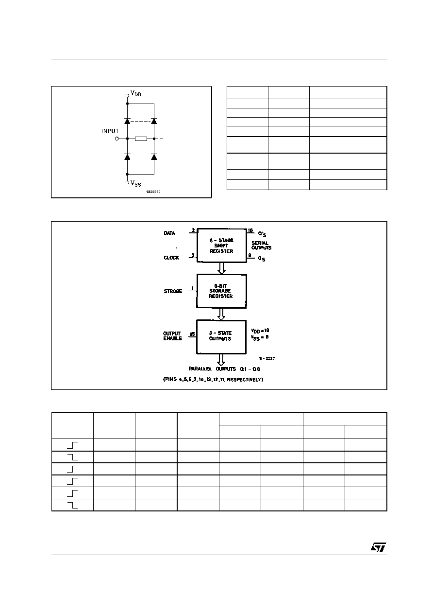
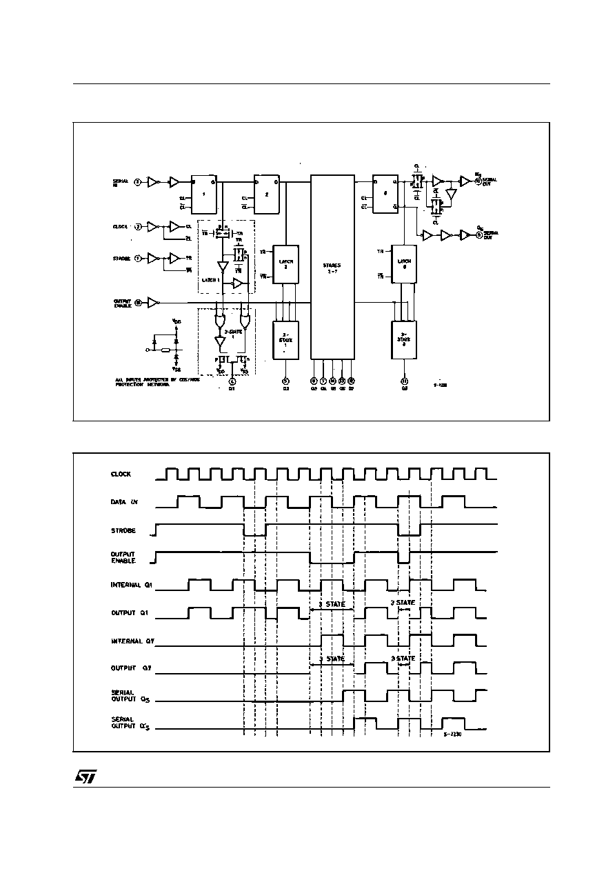
DESCRIPTION
The HCF4094B is a monolithic integrated circuit
fabricated
in
Metal
Oxide
Semiconductor
technology available in DIP and SOP packages.
The HCF4094B is an 8 stages serial shift register
having a storage latch associated with each stage
for strobing data from the serial input to parallel
buffered 3-state outputs. The parallel outputs may
be connected directly to common bus lines. Data
is shifted on positive clock transition. The data in
each shift register stage is transferred to the
storage register when the STROBE input is high.
Data in the storage register appears at the outputs
whenever the OUTPUT-ENABLE signal is high.
Two serial outputs are available for cascading a
number of HCF4094B devices. Data is available
at the Q
S
serial output terminal on positive clock
edges to allow for high speed operation in
cascaded system in which the clock rise time is
fast. The same serial information, available at the
Q'
S
terminal on the next negative clock edge,
provides a means for cascading HCF4094B
devices when the clock rise time is slow.
HCF4094B
8 STAGE SHIFT AND STORE BUS REGISTER
WITH 3-STATE OUTPUTS
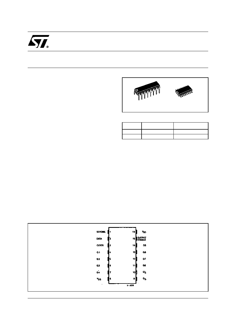
PIN CONNECTION
ORDER CODES
PACKAGE
TUBE
T & R
DIP
HCF4094BEY
SOP
HCF4094BM1
HCF4094M013TR
DIP
SOP
HCF4094B
4/12
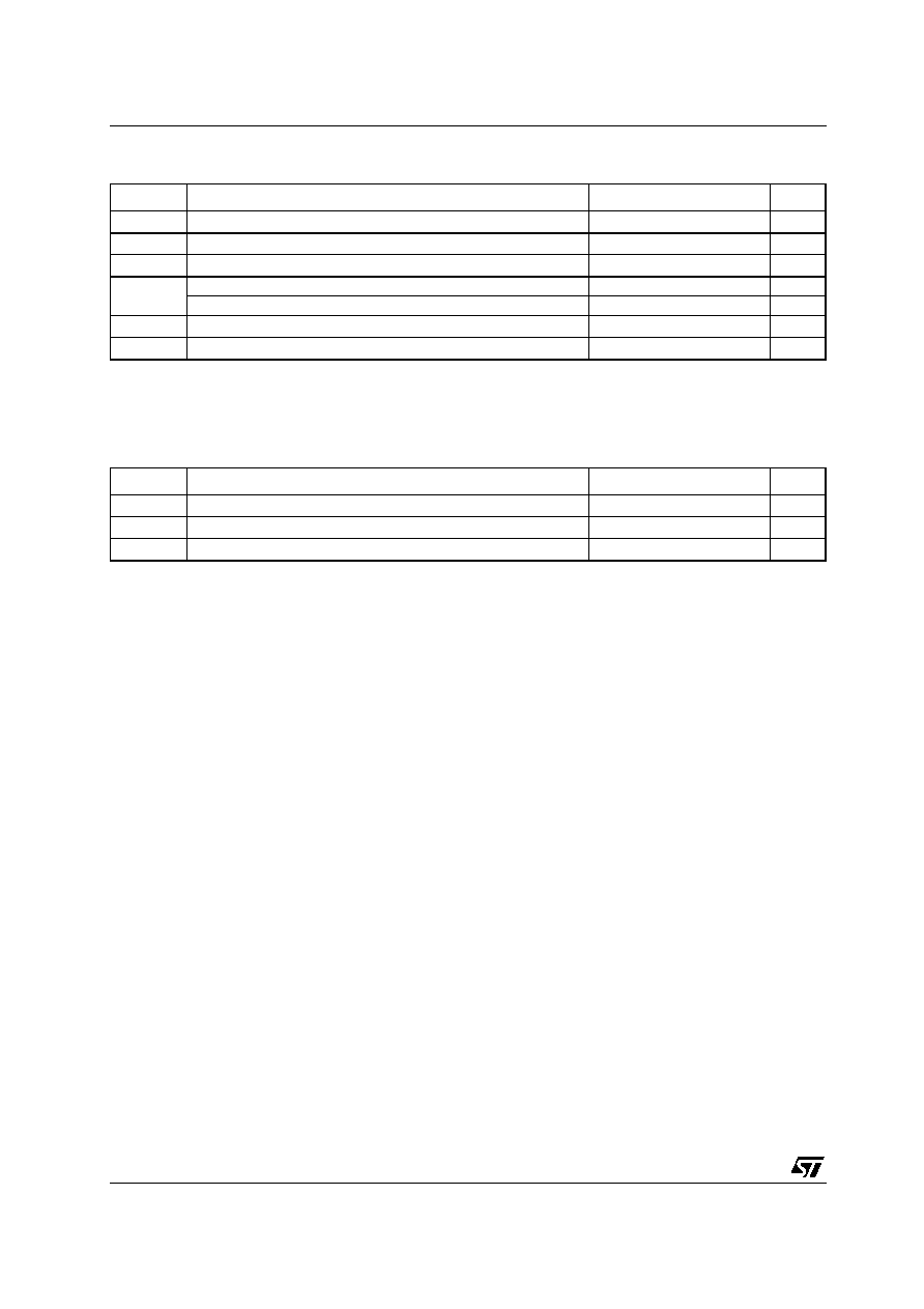
ABSOLUTE MAXIMUM RATINGS
Absolute Maximum Ratings are those values beyond which damage to the device may occur. Functional operation under these conditions is
not implied.
All voltage values are referred to V
SS
pin voltage.
(*) 500mW at 65
į
C; derate to 300mW by 10mW/
į
C from 65
į
C to 85
į
C
RECOMMENDED OPERATING CONDITIONS
Symbol
Parameter
Value
Unit
V
DD
Supply Voltage
-0.5 to +22
V
V
I
DC Input Voltage
-0.5 to V
DD
+ 0.5
V
I
I
DC Input Current
Ī
10
mA
P
D
Power Dissipation per Package
500 (*)
mW
Power Dissipation per Output Transistor
100
mW
T
op
Operating Temperature
-55 to +125
įC
T
stg
Storage Temperature
-65 to +150
įC
Symbol
Parameter
Value
Unit
V
DD
Supply Voltage
3 to 20
V
V
I
Input Voltage
0 to V
DD
V
T
op
Operating Temperature
-55 to 125
įC